This how to will guide you on schematic and PCB design using kiCad
This is a quick guide if you want to start making a simple PCB design for more detailed and comprehensive guide i suggest you to look up kicad documentation: Home | 8.0 | English | Documentation | KiCad
here you’ll find documentation on
schematic Schematic Editor | 8.0 | English | Documentation | KiCad,
PCB PCB Editor | 8.0 | English | Documentation | KiCad
gerber editor and other handy tool
Installing KiCad
it’s a very straight forward process, you can install from the official website: Download | KiCad EDA and follow the installation.
Creating your project
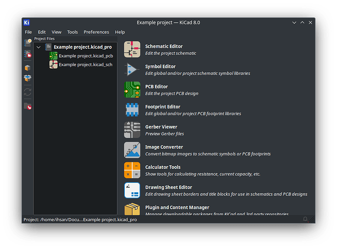
Open kicad > File > New Project… then name your new project.
Creating schematic
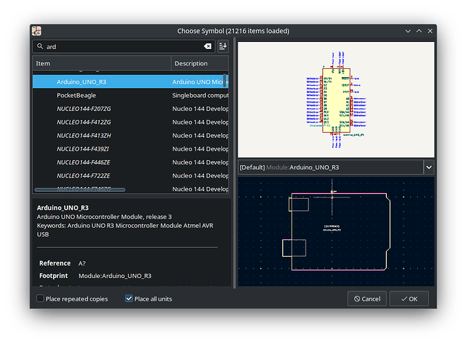
Click on .kicad_sch. next we will be adding our component’s symbol. You can click on Add Symbol or just press A. The symbol library is organized hierarchically, with symbols grouped into libraries based on component type, function, or manufacturer (e.g.,Device,Resistor,Transistor,Microcontroller, etc.).
Footprint
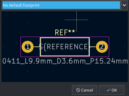
Once you find the correct symbol to your component, you might notice the symbol didn’t have footprint assigned. A footprint is essentially the “blueprint” of where a component will sit and connect on the PCB.
For generic component, you can select the footprint in the dropdown menu. make sure to select footprint with matching dimension to your actual component.
Wiring
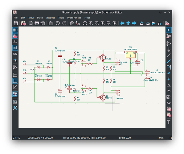
You can choose to wire and add your symbol simultaneously or do the wiring after all symbols are added. Either way after you done, you can proceed to design your PCB. You will be prompted to assign some footprint if you haven’t done so.
PCB Design
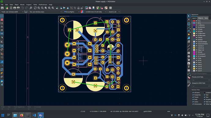
Your objective is to arrange your components’ footprint in such a way that the “wire track” doesnt cross with each other. you will be using the track, drag flip and rotate tool to do so. my tips is to leave the ground and vcc alone, connect anything else first then proceed to do the ground and vcc.
Ground connection (green ratsnest)
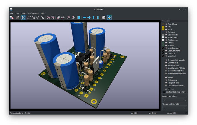
Render on 3D Viewer
hope you find this how-to helpful.
